To start the development of Electronics application there must be a proper circuit diagram and to produce an electronics application as product there must be Designed PCB (Printed Circuit Board).
This Training Module covers the designing of electronics circuits schematics and PCB designing using professional software like ORCAD and Altium (with trial or student version)
Focus Area:
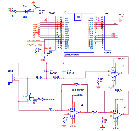
Understanding components symbol library. Component symbol designing.
Practical study of various tools and process used in schematic designing
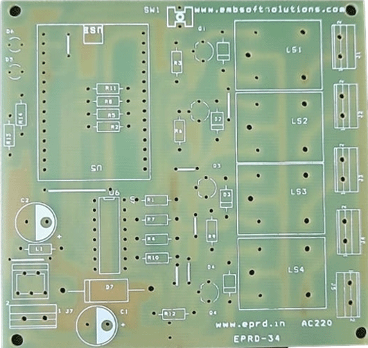
Understanding fundamental concept of PCB designing like footprints,layers, PTH,PCB Trace width selection etc.
Practical study of various PCB Packages of Through hole and SMD components.
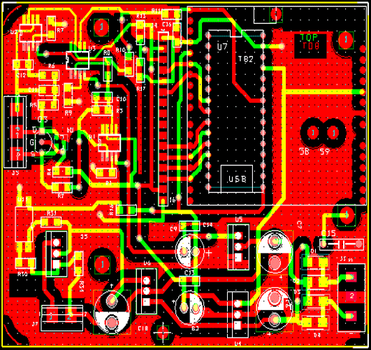
Practical study of various tools and process used in Single to Multi layer PCB designing like component placement, routing,Copper trace width adjustment, Padstack settings, Drill Settings,copper pouring, Placing Fiducials.